

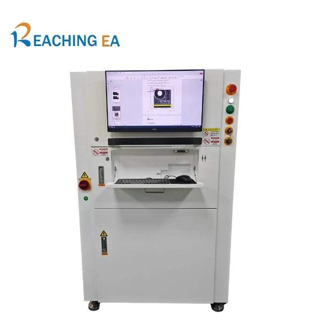
3D Inline SPI
The 3D Inline SPI (3D Solder Paste Inspection) system is a high-precision inline measurement solution designed for modern SMT production lines. Powered by PSLM PMP 3D structured-light technology, high-resolution industrial cameras, and telecentric optics, the system delivers ultra-accurate inspection of solder paste volume, height, area, offset and shape. With fast cycle time, stable repeatability under 1 μm, and full compatibility with MES and printer closed-loop control, this 3D SPI ensures reliable printing quality, reduces defects, and optimizes overall production efficiency. It supports Gerber import, one-click programming, SPC analysis and real-time data reporting, making it an ideal inspection platform for high-density assembly, miniaturized components (01005/008004) and large-volume manufacturing environments.
3D Inline SPI - Key Features
- High-accuracy 3D measurement using PSLM PMP phase-modulation structured-light technology
- Ultra-fast inspection speed (0.35–0.5 sec/FOV) for high-volume SMT lines
- Repeatability ≤1 μm, Gage R&R <10% ensuring stable and reliable measurement
- Supports 01005 / 008004 micro-components and high-density printing
- Telecentric lens + high-pixel CCD for distortion-free image capture
- Real-time SPC & MES connectivity for full-process data control
- Printer closed-loop control to automatically optimize solder paste printing
- Gerber import + easy programming (5-minute setup, one-click operation)
- Dynamic PCB warp compensation up to ±5 mm
- Optional dual-lane & large-panel platforms for flexible production needs
The multi-frequency PSLM technology uses programmable structured light to replace traditional mechanical optical grating cycles, significantly improving measurement accuracy and expanding detection height up to ±1200 μm. By eliminating mechanical drives, the system achieves higher stability, faster response, and lower maintenance costs, making it ideal for high-precision 3D solder paste inspection.

Phase Modulation Profilometry (PMP) enables ultra-high measurement resolution down to 0.37 μm through full-spectrum phase modulation and 4–8× sampling, ensuring exceptional repeatability. Combined with a high-precision ball screw and linear guide rail, it delivers highly accurate and stable 3D inspection results for advanced solder paste measurement.

The high-resolution, high-frame-rate CCD imaging unit enables fast and stable detection of ultra-small components and high-density assemblies such as 008004. With multiple selectable accuracies from 5 μm to 20 μm, it supports diverse inspection requirements while delivering excellent speed, clarity, and reliability for advanced 3D SPI applications.

Uses high-precision telecentric lenses and advanced software algorithms to eliminate lens distortion, squint, and image deformation, significantly improving inspection accuracy and capability. The system also provides industry-leading static compensation for FPC warpage, ensuring stable and reliable 3D SPI measurement performance.

The 2D lamp panel eliminates angle-related RGB color distortion in solder inspection and offers flexible RGB tuning for different PCB colors. It supports various dispensing process tests and greatly enhances repeatability accuracy in height, volume, and area measurements, improving overall inspection performance.

The patented RGB Tune function captures red, green, and blue images and applies a unique filtering algorithm to eliminate false alarms in solder bridge detection and resolve zero-surface uncertainty. At the same time, it delivers accurate 2D/3D solder paste measurements and high-quality imaging, significantly improving inspection reliability and process control.
The high-rigidity steel frame, combined with closed-loop servo control and a high-precision ball screw, ensures high-speed and stable positioning. With an optional linear and high-precision encoder system, the machine can inspect 03015 component pads with ultra-high resolution. Repeatability reaches up to 1 µm, delivering exceptional accuracy for advanced SMT applications.

Technical Parameters
|
Category |
Item |
Specification |
|
Technology Platform |
Standard Type B/C ; Dual-track Type B/C ; Large Platform |
|
|
Series |
S Series / Hero / Ultra / L1200–2K Series |
|
|
Model |
S8080 / S2020 / Hero / Ultra / L1200 / DL1200 / DL1500 / DL2000 |
|
|
Measurement Principle |
3D White Light PSLM; PMP; 2D & 3D Profilometry |
|
|
Measurements |
Volume, Area, Height, Offset, Shape |
|
|
Detection of Defects |
Insufficient tin, Excess paste, Bridging, Offset, Shape defects, Surface contamination |
|
|
Lens Resolution |
4.5µm / 6µm / 8µm / 10µm / 12µm / 15µm / 16µm / 18µm / 20µm |
|
|
Accuracy |
XY Resolution: 10µm |
|
|
Repeatability |
Height: <1µm (4σ) ; Volume/Area: <1% (4σ) |
|
|
Gage R&R |
<10% |
|
|
Inspection Speed |
0.35 sec/FOV (actual depends on configuration) |
|
|
Quantity of Inspection Head |
Standard 1 ; Optional 2 or 3 heads |
|
|
Mark-point Detection Time |
0.3 sec/piece |
|
|
Maximum Measuring Head Height |
±550µm (±1200µm optional) |
|
|
Maximum PCB Warp |
±5mm |
|
|
Minimum Pad Spacing |
80µm / 100µm / 150µm / 200µm (based on configuration) |
|
|
Minimum Element |
01005 / 03015 / 008004 |
|
|
Max PCB Size (X*Y) |
Standard: 450×490mm / 450×520mm / 630×680mm ; Large: 1200×650mm / 1500×500mm / 2000×650mm |
|
|
Conveyor Setup |
Front or Back orbit, Dynamic orbit optional |
|
|
PCB Transfer Direction |
Left-to-Right or Right-to-Left |
|
|
Conveyor Width Adjustment |
Manual & Automatic |
|
|
Engineering Statistics |
Histogram; X-Bar/R-Chart; CPK; Yield; SPI Daily/Weekly/Monthly Reports |
|
|
Gerber & CAD Data Import |
Supported (Gerber 274X/274D, CAD XY, Part No., Package Type) |
|
|
Operating System |
Windows 10 Professional 64-bit |
|
|
Equipment Dimensions & Weight |
Depending on model: 1350–2030mm (W), 1100–1900mm (D), 1450–1850mm (H); 950–2100kg |
|
|
Optional |
Multi-head configurations, SPC software, 1D/2D barcode scanner, UPS |
Product data is for reference only. Please contact us to confirm the latest information.
Hot Tags: 3d solder paste inline inspection, China 3d solder paste inline inspection manufacturers, suppliers, factory, 3D SPI to Reduce Printing Defects, spi machine in smt, solder paste inspection system, Offline 3D SPI Solder Paste Inspection , 3D SPI for Early Defect Prevention, spi smt machine